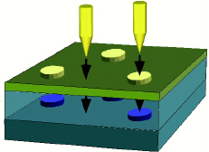
GaSb Self-assembled Quantum Dots on GaAs
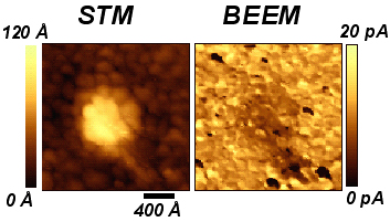
Ballistic elastic electron microscope (BEEM), and scanned tunneling microscope (STM) images of GaSb self-assembled quantum dots on GaAs.
As semiconductor devices approach nanometer dimensions, the development of new electrical measurement tools, particularly for structures buried below the surface, is vital for both scientific understanding and for the development of technology. The original BEEM work was started on NSF MRSEC and STC (QUEST) funding at UCSB. It has been featured in the 1999 NRC report on Condensed Matter and Materials Physics: Basic Research for Tomorrow's Technology. The BEEM apparatus was jointly developed with a small California company, Surface Interface Inc., and this company is now a significant supplier for scanning probe tools. Further development of this tool for simultaneous nanometer, electrical, and optical probing would enhance its utility greatly.
Venky Narayanamurti
Harvard MRSEC (DMR-0820484)